 fig1.GIF
@8k
fig1.GIF
@8kV. Sullivan
Conversion of Apple PCB #820-0014-01 18/02/83
For NTSC Color Video Output
Notes
1) All integrated circuits (ICs), except the ROMs, are referred to by board grid location and pin number. For example B12-05 refers to pin 5 of the IC in row B. column 12. The row and column designations are printed on the top of the board, with the rows being horizontal and the columns being vertical. The ROMs are the six 24 pin chips in row F. They are referred to by their memory address which is printed on the board next to each socket. The six ROMs are DO, D8, ED, E8, FO, and F8.
2) All foil cuts are on the bottom of the board unless otherwise -stated.
3) For cuts on the top of the board, gently lift the black plastic part of the socket with a pair of large pliers or vise-grips, using a slight rocking motion along the long axis of the socket. When the plastic lifts it will leave the pins on the board. The specified cuts can now be made and then the plastic must be carefully pressed back into place BEFORE soldering to the pins. If this is not done the pins will move out of alignment. While the tops of the sockets are off be very careful not to touch the pins. They bend easily and if bent, will give contact problems.
4) The foil cuts may be made with a sharp Xacto knife if you take great care. A much better tool to use would be a small hand grinder, such as a Dremel, with a very small ball mill.
5) All jumper connections are made with #30 wire wrap wire unless otherwise specified.
6) Due to the modifications several of the ICs on the board become spare. These are C11, C2, and E1. Chips must be installed at C2 and E1 as sections of these chips are used during the modifications. No chip should be installed at C11. The socket may be used for the jumper from an additional RAM card if desired.
7) All of these boards were checked at the factory. Some worked and some did not. Those that worked had a written code placed in the white paint square in the upper left hand corner on the top of the board. If your board has no code there I strongly suggest that you look at your board, top and bottom, with a magnifying glass or low power microscope before doing any modifications. What you are locking for are foil bridges where the board was not etched enough, foil opens where the the board was etched too much or solder bridges where too much solder has caused a short circuit between two pins of an IC or Peripheral connector when there was not supposed to be a connection.
8) The modifications are presented in stages. There are several reasons for this:
A) The reasons for doing each modification can be explained.
B) The work can be done at several sittings, minimizing fatigue and thus chances for error.
C) The work can be checked in smaller sections, minimizing the area of the circuit that would have to be checked in case of problems.
D) You may wish not to do some sections of the modifications. Please make the modifications carefully and exactly as presented. A minor error can cause many hours of troubleshooting. Stop and check your work where suggested. If your board does not work find out why before digging yourself in deeper by making more modifications. These mods have been checked-by myself and other people. They have been checked for compatibility with language cards, Z80 cards, Apple disks, and Apple printers so there should be no interface problems. If you have questions consult me before cutting, if you have problems you cannot solve, consult me before cutting further.
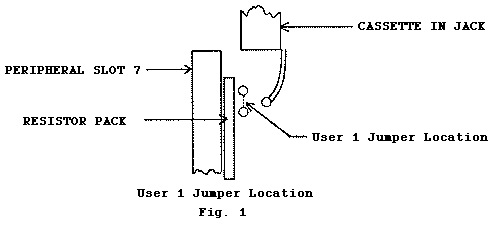
9) The User 1 jumper is shown on page 2 of your schematics. This jumper in not marked in any way on the PCB. It is located as shown in figure 1 below.
fig1.GIF
@8k
10) I would like to thank Kirk Symons of CDC for much information and help, and also Eric Taada for help and moral support. I would also like to thank those of you who waited patiently for me to take the time to do this project properly. Good luck with your board.